SW+ Project Build - Stage 3 The Audio Amplifier
Build instructions by Paul M0BMN
< Previous Next >Stage 3 The Audio Amplifier
in this section we will be building the audio amplifier part of our radio, there are a number of parts used for this stage and I would suggest that you find out all the parts ready first, I have made a list to help.
you may want to print this page off and cross of each part as you fit it.
Parts for the Amplifier (Resistors)
| R2 | 10 K Ohm | Brown Black Orange |
| R3 | 10 K Ohm | as above |
| R4 | 510 K Ohm | Green Brown Yellow |
| R6 | 10 Ohm | Brown Black Black |
| R7 | 510 K Ohm | Green Brown Yellow |
| R8 | 1 M Ohm | Brown Black Green |
| R9 | 4.7 M Ohm | Yellow Violet Green |
| R10 | 22 K Ohm | Red Red Orange |
| R11 | 510 K Ohm | Green Brown Yellow |
| R12 | 1 M Ohm | Brown Black Green |
| R13 | 1 M Ohm | Brown Black Green |
| R14 | 10 Ohm | Brown Black Black |
Now the Capacitors note the Markings are in the 3rd column
| C19 | 0.033uF | '333J' large brown pillow type |
| C20 | 0.1uF | '104' small yellow pillow type |
| C21 | 0.01uF | Ceramic disk marked '103M' |
| C22 | 150pf | Ceramic disk marked '151' or '151J' |
| C23 | 150pf | as above |
| C24 | 0.1uF | '104' small yellow pillow type |
| C25 | 820pf | Ceramic disk marked '821K' or Brown Pillow type |
| C26 | 0.0022uF | '222J' small yellow pillow type |
| C27 | 47uF 16V or 25V | Can Type marked as 47uF 16v/25v, watch which way round you fit this!!!! |
| C106 | 47uF 16V or 25V | as above |
| C107 | 0.1uF | '104' small yellow pillow type |
Now the semiconductors
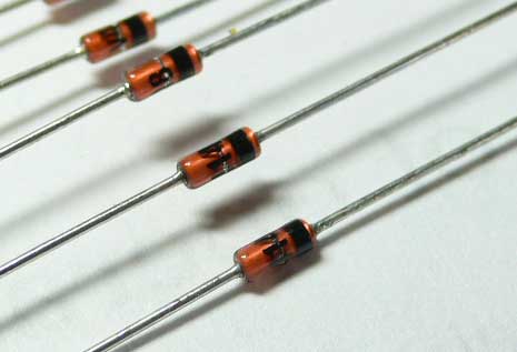
| D3 | 1N4148 | Small Glass diode with brown body, black band at one end |
| D4 | 1N4148 | Small Glass diode with brown body, black band at one end |
| D5 | 1N4148 | Small Glass diode with brown body, black band at one end |
| Q1 | 2N5485 | Field Effect Transistor (FET) layout calls it a MPF102 which is wrong! |
| U4 | NE5532 | 8 pin audio chip IC, fit a 8 pin socket as first before the chip (Supplied) |
Now we have all the parts sorted we can start to build this stage, please pay attention to the instructions, they show where each part is to be located, i would fit the parts in the order of the list above, take care when fitting the electrolytic capacitors c27 and c106, these must be fitted the correct way round, the instruction sheet tells you this too, then be careful with the diodes D3-D5,
they are made from glass and can be broken, also make sure that you fit them the right way round (see the pictures below if unsure)
Note that the layout picture in the instructions shows a MFP102 transistor for Q1, this is a old picture, the MFP102 as been replaced by a new device '2N5485' again make sure you fit this the right way round, make sure that the flat on the body of the transistor is in line with the flat on the outline on the PCB and push the device down so it has about 4-5mm of leads above the board (see photo below) . Be careful with the semiconductors they can be easily damaged by heat and static.
Part1 of Stage 3 The Resistors
These are a easy to fit part, my advice would be to try and make sure that you put them the same way round so the first colour band indicating the value is on top (look at the photos below). you don't need to do that at all and it will work just the same but...if you do have a problem later its easier to read the values if all the resistors are the same way round, and it looks better!, we do want a kit to be proud of don't we.
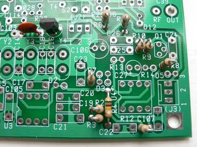 You
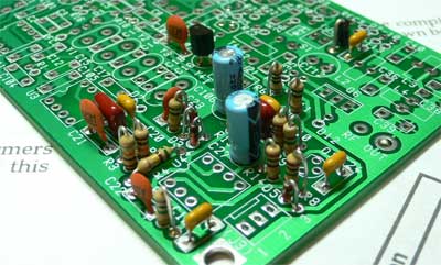
may notice this picture does not have R13 or R14 fitted, I ended up fitting
them after the capcitors , thats because I write the instructions before I build
the stage and then follow them myself to make sure that there right, they are
now!
You
may notice this picture does not have R13 or R14 fitted, I ended up fitting
them after the capcitors , thats because I write the instructions before I build
the stage and then follow them myself to make sure that there right, they are
now!
Now more advice, if you haven't got one go and buy a multi meter, you can get them for much less than £5 or you can pay as much as you like, if this is likely to be the first of many projects i would say go and spend a bit more , around £20-£30 will get you a very nice unit that should last you years.
if you have a meter PLEASE check each resistor with it before you fit it, I nearly fitted a 1K resistor Brown Black Red, where i was intending to fit a 10K one (Brown Black Orange) and if I had not checked each one at fitting stage i would have made a mistake for sure.
If you do make a mistake first thing don't panic, check and double check that you have got it wrong for sure, if you have the main concern must be to protect the PCB, we can get most parts from Maplins but we cant get PCB's. If you have to remove parts you will need a solder sucker or solder wick,
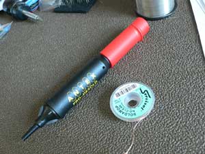
Desoldering Pump and Wick
That's part one done, now part 2 the Capacitors
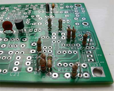
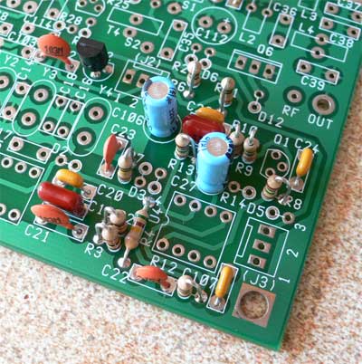
Fit these parts has you did the resistors one by one, check each one before you fit it . with C27 and C106 be extra careful, these devices need to fitted the correct way round, if you look at the case of these you will see that one side is marked - and has a thick black line on it, it also as a shorter leg, this is the negative lead the long lead is the positive, make sure you understand the difference, look at the photo of the board below, that may help too.
 just before I fitted R14! see i make mistooks too!
if you look at your board you will see that one hole for both C26 and C106 have a small + mark by them, the longer lead of these two devices needs to go in this hole, also this is shown in the instructions too that come with the kit.
One more word about fitting these capacitors is like the resistors try and fit the other ones (Not C26/C106) so that the value is readable after the part is fitted (if possible).
Ok Now the Diodes
These are glass be careful not to break them, they are not expensive parts just a few pence each but im sure you dont want to haveto wait a week to get replacments.
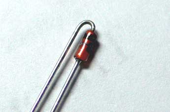
bend the diode leads as shown on the picture on the right above, note the black band is near the bend
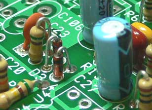
here are the diodes fitted and a closeup showing which way round to fit them
Now onto Q1 and U4 Fitting
Note that the
layout drawing in the instructions shows a MPF102 in the location of Q1 , well
this is a old part and has
been replaced by the newer 2N5485 device. make sure you fit it the right way,
look at the outline on the PCB and the picture below, also fit a 8 pin socket
for the audio chip, make sure you fit that the right way with the small cut
out as per the layout on the PCB again,
When fitting this socket push it in from the top of th eboard and bend over the two outer pins so it doesnt fall out when you solder it in
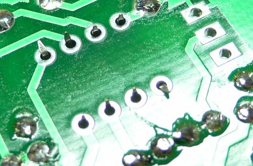 See the bent pins that stop it from falling out when soldering.
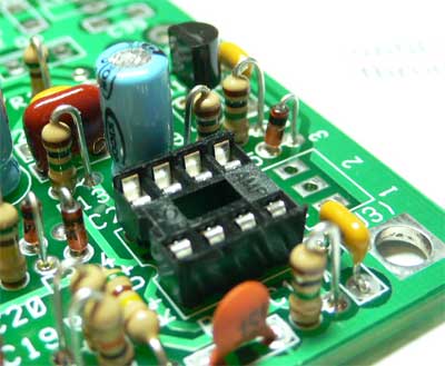
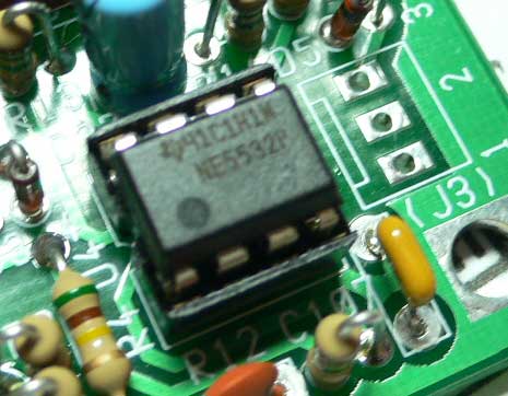
The first picture shows Q1 and the socket fitted, the second shows which way round to fit the audio chip.
Now turn the board over and inspect all the soldering, make sure you have not shorted out any tracks, makes sure all pins are soldered and nice and no dull looking joints, if any do look dry re-solder that joint.
Now take a break, before moving onto the next stage which will be the Crystal Filter/Product Detector/BFO
< Previous Next > Back to SW+ Project Build page